원문대로 에피택셜 웨이퍼
(42)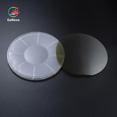
4 인치 4H-SiC 기판 P 레벨 SI 500.0±25.0μm MPD≤5/cm2 저항성≥1E5Ω·cm 전력 마이크로 웨이브
가격: Negotiable
MOQ: Negotiable
배달 시간: 3-4 week days
상표: GaNova
하이 라이트:P 레벨 4H-SiC 기판, 마이크로웨이브 4H-SiC 기판, 4인치 4H-SiC 기판
전력과 마이크로파 소자를 위한 JDCD03-002-002 4 인치 4H-SiC 기판 피-준위 SI 500.0±25.0μm MPD≤5/cm2 Resistivity≥1E5Ω·cm
개관
SiC는 다이오드와 파워 트랜지스터와 고전력 마이크로파 소자와 같은 매우 고전압과 고전력 장치의 제작을 위해 사용됩니다. 전통적 Si 장치와 비교하여, SiC-기반을 둔 전력 소자는 더 빨리 고온 능력 때문에 요구한 교환 속도 더 높은 전압, 더 낮은 저항 성분, 더 작은 크기, 더 적은 냉각을 가집니다.
... 더보기
지금 연락하세요

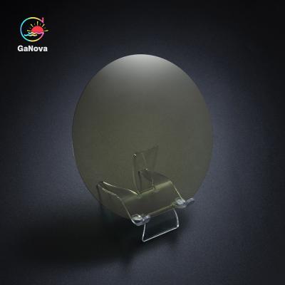
4인치 4H-SiC 기판 P 레벨 SI 500.0±25.0μM MPD≤0.3/Cm2 저항성≥1E9Ω·Cm 전력 마이크로 웨이브
가격: Negotiable
MOQ: Negotiable
배달 시간: 3-4 week days
상표: GaNova
하이 라이트:마이크로웨이브 4H-SiC 기판, 4인치 4H-SiC 기판, 4H-SiC 기판 P 레벨
JDCD03-002-001 4inch 4H-SiC 기판 P-레벨 SI 500.0±25.0μm MPD≤0.3/cm2 Resistivity≥1E9Ω·cm 전력 및 마이크로파 장치용
개요
SiC는 GaAs 또는 Si보다 열 전도율이 높으므로 SiC 장치는 이론적으로 GaAs 또는 Si보다 더 높은 전력 밀도에서 작동할 수 있습니다.넓은 밴드 갭 및 높은 임계 필드와 결합된 더 높은 열 전도율은 SiC 반도체가 높은 전력이 바람직한 주요 장치 기능일 때 이점을 제공합니다.
현재 실리콘 카바이드(SiC)는 고전력 애플리케이션... 더보기
지금 연락하세요
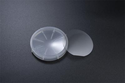
4인치 4H-SiC 기판 P-레벨 N-타입 350.0±25.0μM MPD≤0.5/Cm2 비저항 0.015Ω•Cm—0.025Ω•Cm
가격: Negotiable
MOQ: Negotiable
배달 시간: 3-4 week days
상표: GaNova
하이 라이트:4inch SiC Substrate
4인치 4H-SiC 기판 D-레벨 N-타입 350.0±25.0μm MPD≤5/cm2 저항률 0.015Ω•cm—0.025Ω•cm 전력 및 마이크로웨이브 장치용
개요
고온 장치
SiC는 열전도율이 높기 때문에 다른 반도체 재료보다 더 빨리 열을 발산합니다.이를 통해 SiC 장치는 매우 높은 전력 수준에서 작동할 수 있으며 장치에서 생성된 많은 양의 과도한 열을 여전히 발산할 수 있습니다.
고주파 전력 장치
SiC 기반 마이크로파 전자 장치는 무선 통신 및 레이더에 사용됩니다.
4inch... 더보기
지금 연락하세요
2인치 전력 장치 고전자 이동성 트랜지스터 에피타시얼 웨이퍼
가격: Negotiable
MOQ: 5
배달 시간: Negotiable
상표: Ganova
하이 라이트:sic epitaxial wafer 2 Inch, Power Device sic epitaxial wafer, High Electron Mobility Transistor Epitaxial Wafer
Introduction to GaN on Silicon HEMT Epi wafer Silicon based gallium nitride HEMT epitaxial wafer is a high electron mobility transistor (HEMT) epitaxial wafer based on gallium nitride (GaN) material. Its structure mainly includes AlGaN barrier layer, GaN channel layer, AlN buffer layer, and silicon ... 더보기
지금 연락하세요
2 인치 GaN에 실리콘 HEMT 에피 웨이퍼에 전력 장치
가격: Negotiable
MOQ: 5
배달 시간: Negotiable
상표: Ganova
하이 라이트:GaN On Silicon HEMT Epi Wafer, 2 Inch Epi Wafer, Power Device Epi Wafer
Introduction to GaN on Silicon HEMT Epi wafer Silicon based gallium nitride HEMT epitaxial wafer is a high electron mobility transistor (HEMT) epitaxial wafer based on gallium nitride (GaN) material. Its structure mainly includes AlGaN barrier layer, GaN channel layer, AlN buffer layer, and silicon ... 더보기
지금 연락하세요
알가안 장벽 실리콘 HEMT 에피 웨이퍼 갈륨 나이트라이드 GaN-on-Si에 4 인치 GaN
가격: Negotiable
MOQ: 5
배달 시간: Negotiable
상표: Ganova
하이 라이트:4 inch sic epitaxial wafer, 4 inch sic epi wafer, 4 inch sic epi wafers
Introduction to GaN on Silicon HEMT Epi wafer Silicon based gallium nitride HEMT epitaxial wafer is a high electron mobility transistor (HEMT) epitaxial wafer based on gallium nitride (GaN) material. Its structure mainly includes AlGaN barrier layer, GaN channel layer, AlN buffer layer, and silicon ... 더보기
지금 연락하세요
실리콘 HEMT 에피 웨이퍼 전원 장치에 6 인치 GaN 가륨 질산 GaN Si에
가격: Negotiable
MOQ: 5
배달 시간: Negotiable
상표: Ganova
하이 라이트:6 Inch sic epitaxial wafer, 6 Inch sic epi wafer, 6 Inch sic epi wafers
Introduction to GaN on Silicon HEMT Epi wafer Silicon based gallium nitride HEMT epitaxial wafer is a high electron mobility transistor (HEMT) epitaxial wafer based on gallium nitride (GaN) material. Its structure mainly includes AlGaN barrier layer, GaN channel layer, AlN buffer layer, and silicon ... 더보기
지금 연락하세요
실리콘에 GaN 보라색 레이저 2 인치 실리콘 HEMT 에피 웨이퍼 UV LD 에피 웨이퍼에 GaN
가격: Negotiable
MOQ: 5
배달 시간: Negotiable
상표: Ganova
하이 라이트:2 inch sic epitaxial wafer, 2 inch sic epi wafer, 2 inch sic epi wafers
Introduction to GaN on Silicon HEMT Epi wafer Silicon based gallium nitride HEMT epitaxial wafer is a high electron mobility transistor (HEMT) epitaxial wafer based on gallium nitride (GaN) material. Its structure mainly includes AlGaN barrier layer, GaN channel layer, AlN buffer layer, and silicon ... 더보기
지금 연락하세요
2인치 가너 실리콘 블루 LD 에피 웨이퍼 가너 블루 레이저 실리콘
가격: Negotiable
MOQ: 5
배달 시간: Negotiable
상표: Ganova
하이 라이트:2 inch sic epitaxial wafer, 2 inch sic epi wafer, 2 inch sic epi wafers
Introduction to GaN on Silicon HEMT Epi wafer Silicon based gallium nitride HEMT epitaxial wafer is a high electron mobility transistor (HEMT) epitaxial wafer based on gallium nitride (GaN) material. Its structure mainly includes AlGaN barrier layer, GaN channel layer, AlN buffer layer, and silicon ... 더보기
지금 연락하세요
블루 LED GaN 오브 실리콘 웨이퍼 블루 레이저 GaN 에피타시얼 웨이퍼
가격: Negotiable
MOQ: 5
배달 시간: Negotiable
상표: Ganova
하이 라이트:Silicon Based Gallium Nitride Epitaxial Wafer, HEMT epitaxial wafer, 4 inch sic epitaxial wafer
Introduction to GaN on Silicon HEMT Epi wafer Silicon based gallium nitride HEMT epitaxial wafer is a high electron mobility transistor (HEMT) epitaxial wafer based on gallium nitride (GaN) material. Its structure mainly includes AlGaN barrier layer, GaN channel layer, AlN buffer layer, and silicon ... 더보기
지금 연락하세요
실리콘 녹색 LED 에피 웨이퍼에 2인치 GaN 실리콘에 갈륨 질산
가격: Negotiable
MOQ: 5
배달 시간: Negotiable
상표: Ganova
하이 라이트:2 inch sic epitaxial wafer, 2 inch sic epi wafer, 2 inch sic epi wafers
Introduction to GaN on Silicon Green LED Epi wafer GaN on Silicon Green LED Epi wafer are semiconductor structures formed on silicon substrate materials through epitaxial growth technology for manufacturing green light-emitting diodes (LEDs). It is a key intermediate material in the manufacturing of... 더보기
지금 연락하세요

4인치 GaN 실리콘 그린 LED 에피 웨이퍼 SiC 에피타시얼 웨이퍼
가격: 1000
MOQ: 5
배달 시간: Negotiable
상표: Ganova
하이 라이트:4 inch sic epitaxial wafer, 4 inch sic epi wafer, 4 inch sic epi wafers
Introduction to GaN on Silicon Green LED Epi wafer GaN on Silicon Green LED Epi wafer are semiconductor structures formed on silicon substrate materials through epitaxial growth technology for manufacturing green light-emitting diodes (LEDs). It is a key intermediate material in the manufacturing of... 더보기
지금 연락하세요

4인치 UGaN를 실리콘 비도핑 갈리엄 나이트라이드 위에 실리콘 에피타시얼 웨이퍼
가격: 1000
MOQ: 5
배달 시간: Negotiable
상표: Ganova
하이 라이트:4 inch sic epitaxial wafer, 4 inch sic epi wafer, 4 inch sic epi wafers
Introduction to GaN on Silicon Green LED Epi wafer GaN on Silicon Green LED Epi wafer are semiconductor structures formed on silicon substrate materials through epitaxial growth technology for manufacturing green light-emitting diodes (LEDs). It is a key intermediate material in the manufacturing of... 더보기
지금 연락하세요

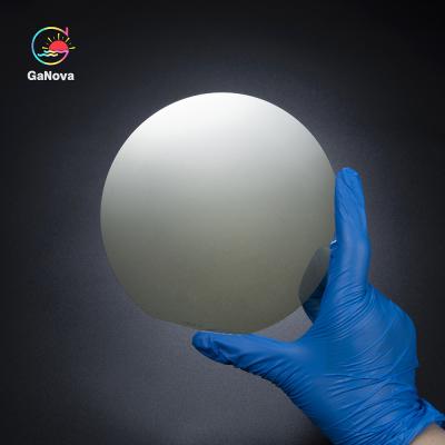
150.0 밀리미터 에피인 +0mm/-0.2mm SiC는 어떤 2차 플래트 3 밀리미터도 웨이퍼로 만들지 않습니다
가격: Negotiable
MOQ: Negotiable
배달 시간: 3-4 week days
상표: GaNova
하이 라이트:150.0 mm SiC Epitaxial Wafer, silicon carbide wafer 3mm, SiC Epitaxial Wafer No Secondary Flat
JDCD03-001-003 Overview SiC boules (crystals) are grown, machined into ingots, and then sliced into substrates, which are subsequently polished. A thin SiC epitaxial layer is then grown on top of this substrate to create an epi-wafer. Today, the semiconductor industry is expanding at a rapid rate, w... 더보기
지금 연락하세요
47.5 밀리미터 ± 1.5 밀리미터 SiC 에피택셜 웨이퍼 150.0 밀리미터 +0mm/-0.2mm은 to<11-20>±1을 평행시킵니다'
가격: Negotiable
MOQ: Negotiable
배달 시간: 3-4 week days
상표: GaNova
하이 라이트:446mm SiC Epitaxial Wafer, 4 H epitaxial silicon wafer, UKAS SiC Epitaxial Wafer
47.5 mm ± 1.5 mm SiC Epitaxial Wafer 150.0 mm +0mm/-0.2mm Parallel to±1° JDCD03-001-003 Overview Currently, there are two main types of SiC wafers. The first type is the polished wafer, which is a single silicon carbide disc. It is made of high-purity SiC crystals, and can be 100mm or 150mm in diame... 더보기
지금 연락하세요

4H SiC 에피택셜 웨이퍼 ≤0.2 /cm2 0.015Ωocm-0.025Ωocm 150.0 밀리미터 +0mm/-0.2mm
가격: Negotiable
MOQ: Negotiable
배달 시간: 3-4 week days
상표: GaNova
하이 라이트:4H SiC Epitaxial Wafer, silicon carbide wafer ISO9001, SiC Epitaxial Wafer 0.2 /Cm2
4H SiC Epitaxial Wafer ≤0.2 /Cm2 0.015Ω•Cm—0.025Ω•Cm 150.0 mm +0mm/-0.2mm JDCD03-001-004 Overview The 200-mm wafers can be used for a variety of applications. These wafers are 50% thinner than the standard silicon wafer, so the 200-mm diameter can be used for more SiC devices. The 200-mm size is muc... 더보기
지금 연락하세요

4H SiC 에피택셜 웨이퍼 0.015Ωocm-0.025ΩoCm ≤4000/cm2150.0 밀리미터 +0mm/-0.2mm
가격: Negotiable
MOQ: Negotiable
배달 시간: 3-4 week days
상표: GaNova
하이 라이트:4H SiC Epitaxial Wafer, silicon epi wafer 0.025Ω•Cm, SiC Epitaxial Wafer 0.015Ω•Cm
4H SiC Epitaxial Wafer 0.015Ω•cm—0.025Ω•cm ≤4000/cm2 150.0 mm +0mm/-0.2mm JDCD03-001-003 Overview The next type is beta silicon carbide. Beta SiC is produced at temperatures higher than 1700 degrees Celsius. Alpha carbide is the most common, and has a hexagonal crystal structure similar to Wurtzite.... 더보기
지금 연락하세요

전력 장치 및 마이크로파 장치용 P 레벨 2인치 SiC 기판
가격: Negotiable
MOQ: Negotiable
배달 시간: 3-4 week days
상표: GaNova
하이 라이트:P Level SiC Substrate, Microwave Devices silicon carbide substrate, 2 Inch SiC Substrate
P-Level 4H-N/SI260um±25um 2-Inch SiC Substrate For Power Devices And Microwave Devices JDCD03-001-001 2-inch SiC substrate P-level 4H-N/SI260μm±25μm for power devices and microwave devices Overview Key features Optimizes targeted performance and total cost of ownership for next generation power elec... 더보기
지금 연락하세요

까다로운 전력 전자 장치를 위한 2인치 SiC 기판 350μm
가격: Negotiable
MOQ: Negotiable
배달 시간: 3-4 week days
상표: GaNova
하이 라이트:2 Inch SiC Substrate, Demanding Power Electronics 2 inch wafer, SiC Substrate 350um
P-Level 2-Inch SiC Substrate 4H-N/SI260μm±25μm For Demanding Power Electronics JDCD03-001-001 2-inch SiC substrate P-level 4H-N/SI260μm±25μm for power devices and microwave devices Overview High crystal quality for demanding power electronics As transportation, energy and industrial markets evolve, ... 더보기
지금 연락하세요