GaN 에피택셜 웨이퍼
(69)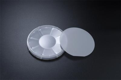
4인치 P형 Mg 도핑된 GaN 사파이어 웨이퍼 SSP 비저항~10Ω Cm LED 레이저 PIN 에피택셜 웨이퍼
가격: Negotiable
MOQ: Negotiable
배달 시간: 3-4 week days
상표: GaNova
하이 라이트:LED Laser PIN Epitaxial Wafer
사파이어 웨이퍼 위의 4인치 P형 Mg 도핑된 GaN SSP 저항률~10Ω cm LED, 레이저, PIN 에피텍셜 웨이퍼
p형 Mg 도핑된 GaN의 전기적 특성은 가변 온도 홀 효과 측정을 통해 조사됩니다.다양한 Mg 도핑 농도를 갖는 샘플은 유기 금속 화학 기상 증착에 의해 준비되었습니다.
도펀트 밀도가 장치 응용 분야에서 일반적으로 사용되는 높은 값으로 증가함에 따라 여러 가지 현상이 관찰됩니다. 유효 억셉터 에너지 깊이가 190에서 112 meV로 감소하고, 저온에서 불순물 전도가 더 두드러지고, 보상 비율이 증... 더보기
지금 연락하세요
Fe는 GaN 기판 Resistivity > 106 Ω·Cm RF 장치에게 도핑했습니다
가격: Negotiable
MOQ: Negotiable
배달 시간: 3-4 week days
상표: GaNova
하이 라이트:ISO GaN Substrates, gan semiconductor wafer, Fe Doped GaN Substrates
2inch C-face Fe-doped SI-type free-standing GaN single crystal substrate Resistivity > 106 Ω·cm RF devices The achieved breakdown voltage of the Fe-doped GaN epitaxial layer can be as high as 2457 V, which is attributed to the Fe-doped GaN epitaxial layer with higher resistance, which can sustain... 더보기
지금 연락하세요
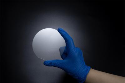
사파이어 빛 SSP 플랫 사파이어 위의 625 um 내지 675 um 4 인치 청색 LED GaN 에피택셜 웨이퍼
가격: Negotiable
MOQ: Negotiable
배달 시간: 3-4 week days
상표: GaNova
하이 라이트:625um GaN Epitaxial Wafer, SSP gan on sapphire wafers, 675um GaN Epitaxial Wafer
Substrate Thickness 650 ± 25 μm 4 Inch Blue LED GaN Epitaxial Wafer On Sapphire SSP Flat Sapphire 4 inch Blue LED GaN epitaxial wafer on sapphire SSP For example, GaN is the substrate which makes violet (405 nm) laser diodes possible, without use of nonlinear optical frequency-doubling. Its sensitiv... 더보기
지금 연락하세요

2 인치 녹색 LED 가온 실리콘 웨이퍼 차원 520±10nm
가격: Negotiable
MOQ: Negotiable
배달 시간: 3-4 week days
상표: GaNova
하이 라이트:실리콘 웨이퍼에 2 인치 가안, 실리콘 웨이퍼에 있는 녹색 LED GaN, 실리콘 웨이퍼에 있는 520nm GaN
실리콘 웨이퍼 위의 2인치 Green-LED GaN
개요
질화 갈륨(GaN)은 전력 전자 분야에서 혁신적인 변화를 일으키고 있습니다.수십 년 동안 실리콘 기반 MOSFET(금속 산화물 반도체 전계 효과 트랜지스터)은 에너지를 전력으로 변환하는 데 도움이 되는 일상적인 현대 세계의 필수적인 부분이었습니다.
GAN(Generative adversarial networks)은 두 개의 신경망을 사용하는 알고리즘 아키텍처로, 실제 데이터를 전달할 수 있는 새로운 합성 데이터 인스턴스를 생성하기 위해 하나를 다른 신경망(따라서 "a... 더보기
지금 연락하세요
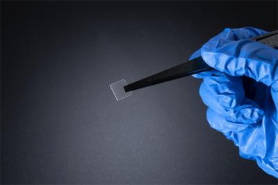
10 X 10.5 mm2 C 얼굴 비 도핑 N 유형 자유 서 있는 GaN 단일 크리스탈 기판
가격: Negotiable
MOQ: Negotiable
배달 시간: 3-4 week days
상표: GaNova
하이 라이트:도핑되지 않은 GaN 단일 크리스탈 기판, 프리-스탠딩 갈륨-질소 단결정체 기판, N형 GaN 단일 결정 기판
10*10.5mm2 C-표면은 n형 프리-스탠딩 갈륨-질소 단결정 기판 저항률을 도프하지 않았습니다 < 0="">
개관
(105 /cm2에 속하여) 저전위 밀도로 최상급 질화갈륨 결정 기판과 어떤 주기성 고장 없이 균일 표면. 이러한 고급 품질 GaN 결정은 90% 이상의 가용 영역을 가지고 있습니다.
우리는 공장으로부터 직접적으로 팔리고, 그러므로 고급 품질 질화갈륨 결정 기판의 시장의 최상의 가격을 제공할 수 있습니다.
10 X 10.5 mm2... 더보기
지금 연락하세요

10*10.5mm2 C-Face Fe-Doped SI형 자유자재 GaN 단일 크리스탈 기판 매크로 결함 밀도 0cm−2 TTV ≤ 10μm 저항성 106 Ω·Cm RF 장치 웨이퍼
가격: Negotiable
MOQ: Negotiable
배달 시간: 3-4 week days
상표: GaNova
하이 라이트:갈륨-질소 단결정체 기판, 10*10.5mm2 GaN 단일 크리스탈 기판
10*10.5mm2 C-표면 철 첨가 SI-타입 자유 고정 갈륨-질소 단결정체 기판 Resistivity > 106 Ω·cm RF 장치 웨이퍼
개관
우리는 공장으로부터 직접적으로 팔리고, 그러므로 고급 품질 질화갈륨 결정 기판의 시장의 최상의 가격을 제공할 수 있습니다. 전 세계에서 고객들은 질화갈륨 결정 기판의 그들의 선호하는 공급자로서 우리의 공급을 믿었습니다.
갈륨 나이트라이드 또는 GaN이 충전기에서 반도체를 위해 사용되기 시작하고 있는 물질입니다. 그것은 90년대에 시작되는 LED를 만드는데 사용되었고 ... 더보기
지금 연락하세요
10 X 10.5 mm2 자유자재 GaN 기판 - 10 μm ≤ BOW ≤ 10 μm
가격: Negotiable
MOQ: Negotiable
배달 시간: 3-4 week days
상표: GaNova
하이 라이트:자유자재로 있는 GaN 기판, 10 x 10.5 mm2 가안 기판
10*10.5mm² C-면 도핑되지 않은 n형 독립형 GaN 단결정 기판 비저항 < 0.1 Ω·cm 전원 장치/레이저
애플리케이션
레이저 다이오드: 보라색 LD, 파란색 LD 및 녹색 LD전력전자기기, 고주파전자기기
GaAs 기판에 대한 10년 이상의 웨이퍼 제조 기술 경험이 GaN 기판 생산에 적용되었습니다.GaN 기판은 손상이 없고 매우 평평하며(Rms < 0.2 nm) 표면 방향이 제어되고 원자 단계 표면이 제어됩니다.에피택셜 성장에 적합한 표면 품질을 달성했습니다.
... 더보기
지금 연락하세요

TTV ≤ 10μm A-Face 무도핑 N형 자유자재 GaN 단일 크리스탈 기판 저항성 0.1 Ω·cm 전력 장치/레이저 W
가격: Negotiable
MOQ: Negotiable
배달 시간: 3-4 week days
상표: GaNova
하이 라이트:레이저 W GaN 싱글 크리스탈 서브스트라트, 전원 장치 GaN 단일 크리스탈 기판, 자유로이 서 있는 GaN 단일 결정 기판
5*10mm2 A-표면은 n형 프리-스탠딩 갈륨-질소 단결정 기판 저항률을 도프하지 않았습니다 < 0="">
개관갈륨 나이트라이드 (GaN)는 단단하고 기계적으로 안정적이 광대역 반도체입니다. 더 높은 항복력, 더 빨리 교환 속도, 높은 열전도율과 더 낮은 온 저항으로, GaN을 기반으로 하는 전력 소자는 의미 심장하게 실리콘 기반 장치를 능가합니다.반도체 물질 갈륨 나이트라이드 (GaN)가 논-톡식과, 인간 세포와 호환 가능합니다 - 물질로 통하는 문이 인 개장이 다양한 생체 의학의 임플란트 기술에 사용한다... 더보기
지금 연락하세요

350 ± 25μm 두께 도핑되지 않은 N형 독립적인 GaN 단일 크리스탈 기판 TTV ≤ 10μm 및 저항성 0.1 Ω·cm
가격: Negotiable
MOQ: Negotiable
배달 시간: 3-4 week days
상표: GaNova
하이 라이트:10μm GaN 단일 크리스탈 기판, 갈륨-질소 단결정체 기판
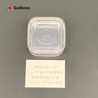
5*10mm2 SP-표면 (20-21)/(20-2-1) 도프하지 않은 n형 프리-스탠딩 갈륨-질소 단결정 기판 저항률 < 0="">
개관갈륨 나이트라이드 (GaN) 기판이 고품질 결정성 기판입니다. 그것은 수년 동안 개발된 원래 원래 HVPE 방식과 웨이퍼 처리 공정 기술로 만들어집니다. 조수석은 높은 수정같은, 좋은 균일성과 뛰어난 표면 품질입니다.
GaN은 그것을 전달하는데 필요한 에너지와 물리적 공간을 줄이는 동안 적용의 넓은 범위에 걸쳐 향상된 성능을 의미 심장하게 제공하기 위해 그것의 능력 때문에 ... 더보기
지금 연락하세요
5*10mm2 SP-Face 10-11 비 도핑 된 N형 독립 GaN 단일 크리스탈 기판 0.1 Ω·cm 전력 장치에 대한 저항성
가격: Negotiable
MOQ: Negotiable
배달 시간: 3-4 week days
상표: GaNova
하이 라이트:0.1 Ω·cm GaN 단일 크리스탈 기판, 5*10mm2 GaN 단일 크리스탈 기판
5*10.5mm2 SP-표면 (10-11) 도프하지 않은 n형 프리-스탠딩 갈륨-질소 단결정 기판 저항률 < 0="">
생성 반대하는 네트워크 (GANs)는 실제 데이터로 통할 수 있는 데이터의 새로운, 종합적 예를 발생시키기 위해 다른 것 (그러므로 반대한 것)에 반대하여 하나를 움푹 들어가면서, 2 신경망을 사용하는 알고리즘 구조입니다. 그들은 화상 생성, 비디오 세대와 음성 발생에 넓게 사용됩니다.
(10-11) 프리-스탠딩 GaN 기판에 직면하세요
항목
... 더보기
지금 연락하세요
5x10mm2 SP-Face 10-11 TTV ≤ 10μm 저항성 0.05 Ω·cm
가격: Negotiable
MOQ: Negotiable
배달 시간: 3-4 week days
상표: GaNova
하이 라이트:프리-스탠딩 갈륨-질소 단결정체 기판, 5x10mm2 GaN 단일 크리스탈 기판
5*10mm2 SP-표면 (10-11) 도프하지 않은 n형 프리-스탠딩 갈륨-질소 단결정 기판 저항률 < 0="">
개관심지어 더 효과적 힘과 더 빨리 더 좋은 회복 특성이면서, GaN은 실리콘 위에서 많은 심각한 이점을 가집니다. 그러나, GaN이 최상의 선택처럼 보일 수 있는 동안 그것은 잠시 모든 애플리케이션에서 실리콘을 대체하고 있지 않을 것입니다.
반 절연 (SI) GaN은 광학적 포논의 제 2 차 고조파 위의 흡수가 발생하는 0.36 um to~7 um으로부터 투명할지 알려져 있습니다.
... 더보기
지금 연락하세요
매크로 결함 밀도 0cm−2 비 도핑된 SI형 자립 GaN 단일 크리스탈 기판 RF 장치 5*10mm2 M면
가격: Negotiable
MOQ: Negotiable
배달 시간: 3-4 week days
상표: GaNova
하이 라이트:RF 장치 GaN 단일 크리스탈 기판, 5*10mm2 GaN 단일 크리스탈 기판, 자유로이 서 있는 GaN 단일 결정 기판
5*10mm2 M-표면은 SI-타입 프리-스탠딩 갈륨-질소 단결정체 기판 Resistivity > 106 Ω·cm RF 장치 웨이퍼를 도프하지 않았습니다
개관딘 epi 웨이퍼는 모서리 MOS 장치를 이깨서 일반적으로 사용됩니다. 두꺼운 Epi 또는 다층 구조 에피택셜 웨이퍼는 전력을 제어하기 위해 주로 장치를 위해 사용되고 그들이 에너지 소비의 효율을 향상시키는데 기여하고 있습니다.
갈륨 나이트라이드 (GaN) 기판이 고품질 결정성 기판입니다. 그것은 수년 동안 개발된 원래 원래 HVPE 방식과 웨이퍼 처리 공정 ... 더보기
지금 연락하세요

SP-Face 11-12 도핑되지 않은 N형 독립 GaN 단일 결정 기판 저항성 0.05 Ω·cm 매크로 결함 밀도 0cm−2
가격: Negotiable
MOQ: Negotiable
배달 시간: 3-4 week days
상표: GaNova
하이 라이트:00, 05 Ω·cm GaN 단일 결정 기판, 도핑되지 않은 GaN 단일 크리스탈 기판
5*10mm2SP-면(11-12) 도핑되지 않은 n형 독립형 GaN 단결정 기판 비저항 < 0.05Ω·cm 전력 장치/레이저 웨이퍼
개요GaN 트랜지스터는 실리콘 트랜지스터보다 빠르게 켜질 수 있기 때문에 이러한 전환으로 인한 손실을 줄일 수 있습니다.GaN이 스위칭 손실을 줄이는 또 다른 방법은 바디 다이오드가 없는 것입니다.
GaN은 기존 실리콘 기술과 비교할 때 성능을 제공하는 데 필요한 에너지와 물리적 공간을 줄이면서 광범위한 응용 분야에서 크게 향상된 성능을 제공할 수 있기 때문에 중요성이 커지고 있습니다.... 더보기
지금 연락하세요

전력장치 5x10mm2 도핑되지 않은 N형 자유자재 GaN 단일 크리스탈 기판, 저항성 0.1 Ω·cm 및 10μm 내의 BOW
가격: Negotiable
MOQ: Negotiable
배달 시간: 3-4 week days
상표: GaNova
하이 라이트:0.1 Ω·cm GaN 단일 크리스탈 기판, 10μm GaN 단일 크리스탈 기판, 5x10mm2 GaN 단일 크리스탈 기판
5*10mm2 SP-표면 (11-12) 도프하지 않은 n형 프리-스탠딩 갈륨-질소 단결정 기판 저항률 < 0="">
개관1990년대 이후로, 그것은 발광 다이오드 (LED)에서 일반적으로 사용되었습니다. 갈륨 나이트라이드는 블루 레이에서 디스크 판독을 위해 사용된 푸른 빛을 내보냅니다. 덧붙여, 갈륨 나이트라이드는 반도체 전력 소자, RF 성분, 레이저와 포토닉스에서 사용됩니다. 미래에, 우리는 센서기술에서 GaN을 볼 것입니다.
(11-22) 프리-스탠딩 GaN 기판에 직면하세요
... 더보기
지금 연락하세요
5*10mm2 SP-Face 비 도핑 N형 자유 서 있는 GaN 단일 크리스탈 기판 20-21 / 20-2-1 10mm2 저항성 0.05 Ω·cm
가격: Negotiable
MOQ: Negotiable
배달 시간: 3-4 week days
상표: GaNova
하이 라이트:00, 05 Ω·cm GaN 단일 결정 기판, 10mm2 GaN 단일 크리스탈 기판, 20-21 GaN 단일 결정 기판
5*10mm2 SP-표면 (20-21)/(20-2-1) 도프하지 않은 n형 프리-스탠딩 갈륨-질소 단결정 기판 저항률 < 0="">
개관생성 반대하는 네트워크 (GAN)는 두 파트를 가집니다 : 생성기는 그럴 듯한 데이터를 만들어내는 것을 배웁니다. 생성된 사례는 판별기를 위해 부정적 훈련 예가 됩니다. 판별기는 실제 데이터와 생성기의 가짜 데이터를 구별하는 것을 배웁니다.
(20-21)/(20-2-1) 표면 프리-스탠딩 GaN 기판
항목
간-FS-SP-U-S
... 더보기
지금 연락하세요
실리콘 웨이퍼 20nmContact 층 위의 차원 520±10nm 2 인치 녹색 LED GaN
가격: Negotiable
MOQ: Negotiable
배달 시간: 3-4 week days
상표: GaNova
하이 라이트:20nm GaN On Silicon Wafer, 520±10nm GaN On Silicon Wafer
실리콘 웨이퍼 위의 2 인치 녹색 LED GaN
개관
갈륨 나이트라이드 (GaN)는 파워 전자 장치 세계 전체에 걸쳐 혁신적 이동을 만들고 있습니다. 수십년간, 실리콘-기반 MOSFET (금속 산화 반도체 FET)는 힘으로 에너지를 변환하는 것을 돕는 매일 현대 세계의 일체형 부품이었습니다.
생성 반대하는 네트워크 (GANs)는 실제 데이터로 통할 수 있는 데이터의 새로운, 종합적 예를 발생시키기 위해 다른 것 (그러므로 반대한 것)에 반대하여 하나를 움푹 들어가면서, 2 신경망을 사용하는 알고리즘 구조입니다. 그들은... 더보기
지금 연락하세요

실리콘 웨이퍼 장황한 부분 D'Onde 레이저 455±10nm 위의 2 인치 블루-LED GaN
가격: Negotiable
MOQ: Negotiable
배달 시간: 3-4 week days
상표: GaNova
하이 라이트:455±10nm GaN On Silicon Wafer
실리콘 웨이퍼 위의 2 인치 블루-LED GaN
갈륨 나이트라이드는 고전력, 고주파 반도체 적용을 위해 사용된 반도체 기술입니다. 갈륨 나이트라이드는 다양한 고전력 요소를 위해 비소화 갈륨과 실리콘 보다 그것을 더 잘 하는 여러 특징을 보여줍니다. 이러한 특성은 더 높은 항복 전압과 더 좋은 전기 고유 저항을 포함합니다.
실리콘 위의 2 인치 GaN 청색 레이저
항목
SI(111) 기판
Al(Ga)N 버퍼
우간
엔간
AlGaN
... 더보기
지금 연락하세요

2인치 C-Face Fe 도핑 SI 유형 독립형 GaN 단결정 기판 저항률 > 10⁶ Ω·cm RF 장치
가격: Negotiable
MOQ: Negotiable
배달 시간: 3-4 week days
상표: Nanowin
하이 라이트:2inch GaN Single Crystal Substrate, Resistivity GaN Single Crystal Substrate
2인치 C면 Fe 도핑 SI형 독립형 GaN 단결정 기판 비저항 > 106Ω·cm RF 장치
개요
질화갈륨(GaN) 에피택셜 웨이퍼(에피 웨이퍼).실리콘 기판, 사파이어 기판, 실리콘 카바이드(SiC) 기판과 같은 다양한 기판의 GaN 고전자 이동도 트랜지스터(HEMT) 웨이퍼.우리는 RF 및 전력 애플리케이션을 위한 SiC 웨이퍼 상의 GaN을 제공합니다.
2인치 독립형 U-GaN/SI-GaN 기판
엑설런트 레벨(S)
... 더보기
지금 연락하세요

4-인치 마그네슘 도프된 GaN/Sapphire 기판 SSP Resistivity~10Ω cm LED 레이저 핀 에피택셜 웨이퍼
가격: Negotiable
MOQ: Negotiable
배달 시간: 3-4 week days
상표: GaNova
하이 라이트:LED Laser GaN Epitaxial Wafer
사파이어 웨이퍼 SSP resistivity~10Ω cm LED, 레이저, 핀 에피택셜 웨이퍼 위의 4 인치 p-형 마그네슘 도핑 갈륨-질소
질화 갈륨 기판을 사용합니까?
사파이어 위의 갈륨 나이트라이드는 라디오 에너지 증폭에 쓸 이상적인 소재입니다. 더 높은 항복 전압과 고온에 있는 더 좋은 성능을 포함하여 그것은 실리콘 위에서 수많은 혜택을 제공합니다.
GaN은 이원 III/V 직접적인 밴드 갭 반도체가 일반적으로 1990년대 이후로 밝은 발광 다이오드에 사용했다는 것 입니다. 합성물은 섬유아연석 결정 구조... 더보기
지금 연락하세요
4인치 N형 UID 도핑된 GaN 사파이어 웨이퍼 SSP 비저항>0.5 Ω cm LED, 레이저, PIN 에피택셜 웨이퍼
가격: Negotiable
MOQ: Negotiable
배달 시간: 3-4 week days
상표: GaNova
하이 라이트:PIN GaN On Sapphire Wafer, 4 Inch GaN On Sapphire Wafer
사파이어 웨이퍼의 4인치 N형 UID 도핑 GaN SSP 저항 >0.5 Ω cm LED, 레이저, PIN 에피택셜 웨이퍼
예를 들어, GaN은 비선형 광학 주파수 배가를 사용하지 않고도 보라색(405nm) 레이저 다이오드를 가능하게 하는 기판입니다.이온화 방사선에 대한 감도가 낮아(다른 III족 질화물과 마찬가지로) 위성용 태양 전지 어레이에 적합한 소재입니다.군사 및 우주 응용 프로그램은 장치가 방사선 환경에서 안정성을 보여줌으로써 이점을 얻을 수 있습니다.
4인치 도핑되지 않은 GaN/사... 더보기
지금 연락하세요