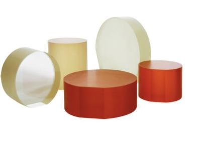
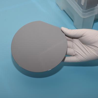
반도체 기질
(95)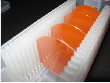
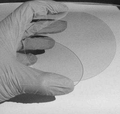
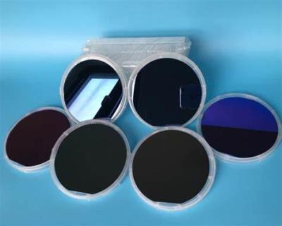
2 인치 갈륨 인화물 수정같은 기질 간격 웨이퍼 0.3 간격은 표면을 쌓았습니다
가격: BY CASE
MOQ: 5PCS
배달 시간: 2-4weeks
상표: zmkj
하이 라이트:웨이퍼 기질, 반도체 웨이퍼
2-6 inch Gallium phosphide (GaP) crystals crystal substrate,GaP wafer ZMKJ can provides 2inch GaP wafer – gallium Phosphide which are grown by LEC(Liquid Encapsulated Czochralski) as epi-ready or mechanical grade with n type, p type or semi-insulating in different orientation(111)or(100). Gallium ph... 더보기
➤ 방문 웹사이트
BAW Devices Dia 50.8mm 1인치 AlN 질화 알루미늄 웨이퍼
가격: by case
MOQ: 1pcs
배달 시간: in 30days
상표: ZMKJ
하이 라이트:AlN 질화 알루미늄 웨이퍼, 50.8mm 질화 알루미늄 웨이퍼, BAW Devices AlN 웨이퍼
dia50.8mm 2inch 1inch AlN substrate/AlN single crystal wafers 10x10mm or diameter 10mm dia25.4mm dia30mm, dia45mm, dia50.8mm AlN substrate AlN single crystal wafers Applications of AlN template we have developed a serials of proprietary processes and technologies to fabricate high-quality AlN templa... 더보기
➤ 방문 웹사이트

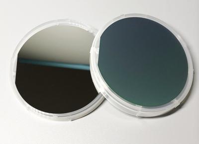
실리콘 기질에 900nm 4 인치 LiNbO3 리튬 니오브산염 웨이퍼 박막 층
가격: by case
MOQ: 2pcs
배달 시간: in 30days
상표: ZMKJ
하이 라이트:LiNbO3 리튬 니오베이트 웨이퍼, 4인치 리튬 니오베이트 웨이퍼, 절연체에 900nm 리튬 니오베이트
4inch 6inch 300-900 nm Lithium Niobate LiNbO3 LN Thin Films (LNOI) on silicon wafer Direction of application: · Electro-Optic Modulators · Delay Lines · Electro-Optic Q Switches · X-BAR · Phase Modulator Devices · Nonlinear Optics · Ferroelectric Memory Devices Characteristic Specification 300-900 n... 더보기
➤ 방문 웹사이트
산업 반도체 기질 S Fe Zn에 의하여 진한 액체로 처리되는 InP 인듐 인화물 단결정 웨이퍼
가격: by case
MOQ: 3pcs
배달 시간: 2-4weeks
상표: zmkj
하이 라이트:gasb substrate, wafer substrate
2inch/3inch/4inch S/Fe/Zn doped InP Indium Phosphide Single Crystal Wafer Indium phosphide (InP) is an important compound semiconductor material with the advantages of high electronic limit drift speed, good radiation resistance and good thermal conductivity. Suitable for manufacturing high frequenc... 더보기
➤ 방문 웹사이트
2-6 인치 반도체 기질 LiNbO3 단결정 기질 웨이퍼
가격: by case
MOQ: 25pcs
배달 시간: 2-4weeks
상표: zmkj
하이 라이트:wafer substrate, semiconductor wafer
4inch diameter 100mm Lithium niobate LiNbO3 substrate wafer, LN wafer for saw and optical,SAW Grade LiNbO3 Crystal ingot Description: Lithium niobate (LiNbO3) is a ferroelectric material suitable for a variety of applications. Its versatility is made possible by the excellent electro-optic, nonline... 더보기
➤ 방문 웹사이트
Y-42° LT 리튬 Tantalate LiTaO3 결정, Fe+는 300um 기질 웨이퍼를을 위한 보았습니다 광학을 진한 액체로 처리했습니다
가격: by case
MOQ: 25pcs
배달 시간: 2-4weeks
상표: zmkj
하이 라이트:wafer substrate, semiconductor wafer
2inch/3inch/4inch/6inch Y-42°/36°/128° LT Lithium tantalate (LiTaO3) crystal / Fe+ doped type 250um/300um substrate wafer Product Name:Lithium tantalate (LiTaO3) crystal substrateProduct Description:Lithium tantalate (LiTaO3) single crystal has a very good electro-optical, piezoelectric and pyroelec... 더보기
➤ 방문 웹사이트
5G 벌크 탄성파 소자를 위한 6 인치 사파이어 기반을 둔 AlN 템플릿 웨이퍼
가격: by case
MOQ: 5pcs
배달 시간: in 30days
상표: ZMKJ
하이 라이트:Sapphire based AlN templates, 6 Inch sapphire wafer, 6 Inch AlN templates
2inch 4iinch 6Inch Sapphire based AlN templates AlN film on sapphire substrate sapphire window sapphire wafer Applications of AlN template Silicon-based semiconductor technology has reached its limits and could not satisfy the requirements of future electronic devices. As a typical kind of 3rd/4th-g... 더보기
➤ 방문 웹사이트
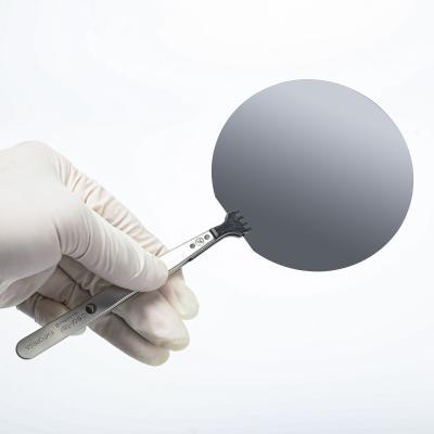
6 인치 앤형 연마 실리콘 웨이퍼 DSP SiO2 실리콘 옥사이드웨이퍼
가격: by quantites
MOQ: 25pcs
배달 시간: 1-4weeks
상표: ZMSH
하이 라이트:N Type Polished Silicon Wafer, SiO2 Silicon Oxide Wafer, DSP Polished Silicon Wafer
6inch 8inch 2inch 1inch FZ CZ N-type polished silicon wafer DSP SiO2 wafers Silicon oxide wafer Polished Silicon Wafer High-purity (11N) 1-12 inch single- and double-polished Czochralski wafers Sizes 1" 2" 3" 4" 5" 6" 8" 12" and special size and specification ... 더보기
➤ 방문 웹사이트
적외선 이산화 탄소 레이저를 위한 4 인치 게르마늄 반도체 기판 Ge 웨이퍼
가격: by specification
MOQ: 3PCS
배달 시간: 2-4weeks;
상표: ZMSH
하이 라이트:Germanium Semiconductor Substrate, Ge Wafers Germanium Substrate, Co2 Lasers Silicon Wafer Substrate
4inch N-type Ge wafers Germanium substrate Ge window for infrared Co2 lasers Ge Material Introduce Among optical materials, germanium materials are increasingly widely used in infrared and night vision technologies. Germanium belongs to the IV main group element and has a diamond structure. Germaniu... 더보기
➤ 방문 웹사이트
적외선 이산화 탄소 레이저를 위한 10 um Ga 도핑된 게르마늄 기판 Ge 윈도우
가격: by specification
MOQ: 3PCS
배달 시간: 2-4weeks;
상표: ZMSH
하이 라이트:Ga Doped Germanium Substrate, 10um Germanium Lenses, Ge Window For Infrared Co2 Lasers
4inch N-type Ge wafers Germanium substrate Ge window for infrared Co2 lasers Ge Material Introduce Among optical materials, germanium materials are increasingly widely used in infrared and night vision technologies. Germanium belongs to the IV main group element and has a diamond structure. Germaniu... 더보기
➤ 방문 웹사이트
10x10mm 전자 주사 현미경 P 유형 실리콘 웨이퍼 사각형 피스 SEM
가격: by quantites
MOQ: 25pcs
배달 시간: 1-4weeks
상표: ZMSH
하이 라이트:Electron Microscope Silicon Wafer Substrates, 10x10mm P Type Silicon Wafer, Square Polished Silicon Wafer
2inch 3inch 4inch 5inch 6inch 8inch 12inch FZ CZ N-type polished silicon wafer DSP SiO2 wafers Silicon oxide wafer 1inch 2inch 10x10mm Scanning electron microscope silicon wafer small square piece SEM Polished Silicon Wafer High-purity (11N) 1-12 inch single- and double-polished Czochralski wafers S... 더보기
➤ 방문 웹사이트
Dia 50.8 밀리미터 Ge 웨이퍼 반도체 기판 Ga 도핑된 기판 엔은 500 um을 타이핑합니다
가격: by case
MOQ: 5pcs
배달 시간: 2-4weeks
상표: zmkj
하이 라이트:N Type GaAs Epi Wafer, Ga Doped Silicon Wafer Substrate, Ge Wafers Silicon Substrate
2INCH dia50.8mm Ga doped Ge substrate 4inch N-type 500um Ge wafers Ge wafer for microelectronic application N type, Sb doped Ge wafer N type,undoped Ge wafer P type,Ga doped Ge wafer Available size:2”-6” Available orientation: (100),(111),or custom specs. Available grade: IR grade, electronic grade ... 더보기
➤ 방문 웹사이트
OEM Dia 25.4 밀리미터 단일 결정 Ge 광학렌즈
가격: by case
MOQ: 10pcs
배달 시간: 2-4weeks
상표: zmkj
하이 라이트:단결정 질화 갈륨 웨이퍼, Dia 25.4 밀리미터 갈륨 질화물 웨이퍼, OEM 갈륨 질화물 웨이퍼
dia25.4mm Ge windows Single Crystal Germanium Ge Wafer for Semiconductor device Product Description ZMKJ is a worldwide supplier of single crystal Germanium lens and single crystal Ge ingot , we have a strong advantage in providing single crystal wafer to micro-electronics and opto-electronics indus... 더보기
➤ 방문 웹사이트
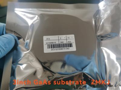
열벽 증착기를 위한 VGF 6 인치 앤형 갈륨 비소 반도체 기판
가격: BY case
MOQ: 3PCS
배달 시간: 2-6weeks
상표: ZMSH
하이 라이트:갈륨 비소 반도체 기판, VGF 반도체 기판, 열벽 증착기 n 형 기판
VGF 2inch 4inch 6inch n-type prime grade GaAs wafer for epitaxial growth GaAs wafer (Gallium Arsenide) is an advantageous alternative to silicon that has been evolving in the semiconductor industry. Less power consumption and more efficiency offered by this GaAs wafers are attracting the market play... 더보기
➤ 방문 웹사이트

2 인치 1000nm 알루미늄질화물 필름 실리콘 기반을 둔 알루미늄 질화물 반도체 기판
가격: by case
MOQ: 3pcs
배달 시간: in 30days
상표: ZMKJ
하이 라이트:AlN 필름 반도체 기판, AlN 질화 알루미늄 기판, 1000nm 질화 알루미늄 웨이퍼
4inch 6inch Silicon-based AlN templates 500nm AlN film on silicon substrate Applications of AlN template Silicon-based semiconductor technology has reached its limits and could not satisfy the requirements of future electronic devices. As a typical kind of 3rd/4th-generation semiconductor material, ... 더보기
➤ 방문 웹사이트

4 " 사파이어 기반을 둔 gan 템플릿 반도체 기판
가격: by case
MOQ: 5pcs
배달 시간: in 30days
상표: ZMKJ
하이 라이트:5G 톱 gan 템플릿, 4" gan 템플릿, GaN 반도체 기판
2inch 4inch 4" Sapphire based GaN templates GaN film on sapphire substrate Properties of GaN Chemical properties of GaN 1) At room temperature, GaN is insoluble in water, acid and alkali. 2)Dissolved in a hot alkaline solution at a very slow rate. 3) NaOH, H2SO4 and H3PO4 can quickly corrode th... 더보기
➤ 방문 웹사이트
6 " 실리콘은 AlN 템플릿 500nm 알루미늄질화물 필름을 실리콘 기판에 바탕을 두었습니다
가격: by case
MOQ: 3pcs
배달 시간: in 30days
상표: ZMKJ
하이 라이트:실리콘 기판의 AlN 필름, 500nm AlN 템플릿, 6" AlN 템플릿
diameter 150mm 8inch 4inch 6inch Silicon-based AlN templates 500nm AlN film on silicon substrate Applications of AlN template Silicon-based semiconductor technology has reached its limits and could not satisfy the requirements of future electronic devices. As a typical kind of 3rd/4th-generation sem... 더보기
➤ 방문 웹사이트

30 밀리미터 Dia AlN 단-결정 반도체 기판
가격: by case
MOQ: 3pcs
배달 시간: in 30days
상표: ZMKJ
하이 라이트:AlN 반도체 기판, 30mm 직경 aln 기판, 30mm aln 단결정
diameter 150mm 8inch 4inch 6inch Silicon-based AlN templates 500nm AlN film on silicon substrate Applications of AlN template Silicon-based semiconductor technology has reached its limits and could not satisfy the requirements of future electronic devices. As a typical kind of 3rd/4th-generation sem... 더보기
➤ 방문 웹사이트
5G 톱 직경 10mm 단결정 AlN 반도체 기판
가격: by case
MOQ: 1pcs
배달 시간: in 30days
상표: ZMKJ
하이 라이트:직경 10mm Aln 기판, 5G 톱 반도체 기판, 단결정 Aln 기판
10x10mm or diameter 10mm dia25.4mm dia30mm, dia45mm, dia50.8mm AlN substrate AlN single crystal wafers Applications of AlN template Silicon-based semiconductor technology has reached its limits and could not satisfy the requirements of future electronic devices. As a typical kind of 3rd/4th-generati... 더보기
➤ 방문 웹사이트
4인치 N형 15° 반도체 기판 Si 도핑된 GaAs 웨이퍼 SSP
가격: 100-200usd/pcs
MOQ: 5pcs
배달 시간: 2-4weeks
상표: zmkj
하이 라이트:Si 도핑된 GaAs 웨이퍼, 반도체 기판 GaAs 웨이퍼, N형 ssp 웨이퍼
VFG metod N-type 2inch/3inch,4inch ,6inch dia150mm GaAs Gallium Arsenide Wafers N-type Semi-insulating type for Microelectronics, --------------------------------------------------------------------------------------------------------------(GaAs) Gallium Arsenide WafersGallium arsenide (GaAs) is a c... 더보기
➤ 방문 웹사이트